
Schottky Diodes
Schottky diodes are named after their inventor, Dr. Schottky. SBD is the abbreviation of Schottky Barrier Diode (Schottky Barrier Diode, abbreviated as SBD). SBD is not made by the principle of forming a PN junction by contacting a P-type semiconductor and an N-type semiconductor, but by using the p
Schottky diodes are named after their inventor, Dr. Schottky. SBD is the abbreviation of Schottky Barrier Diode (Schottky Barrier Diode, abbreviated as SBD). SBD is not made by the principle of forming a PN junction by contacting a P-type semiconductor and an N-type semiconductor, but by using the principle of a metal-semiconductor junction formed by the contact between a metal and a semiconductor. Therefore, SBD is also called metal-semiconductor (contact) diode or surface barrier diode, which is a type of hot carrier diode.

Schottky's principle
Schematic diagram of Schottky diode structure
A Schottky diode is a metal-semiconductor device made of a noble metal (gold, silver, aluminum, platinum, etc.) A as the positive electrode and an N-type semiconductor B as the negative electrode, and the potential barrier formed on the contact surface of the two has rectification characteristics. Because there are a large number of electrons in the N-type semiconductor and only a small amount of free electrons in the noble metal, the electrons diffuse from B with high concentration to A with low concentration. Obviously, there are no holes in metal A, and there is no diffusion of holes from A to B. As electrons continue to diffuse from B to A, the electron concentration on the surface of B gradually decreases, and the surface electrical neutrality is destroyed, thus forming a potential barrier, and its electric field direction is B→A. However, under the action of the electric field, the electrons in A will also produce a drift motion from A→B, thus weakening the electric field formed due to the diffusion motion. When a space charge region of a certain width is established, the electron drift movement caused by the electric field and the electron diffusion movement caused by different concentrations reach a relative balance, forming a Schottky barrier.
The internal circuit structure of a typical Schottky rectifier is based on an N-type semiconductor substrate, on which an N-epitaxial layer with arsenic as a dopant is formed. The anode uses materials such as molybdenum or aluminum to make the barrier layer. Silicon dioxide (SiO2) is used to eliminate the electric field in the edge area and improve the withstand voltage value of the tube. The N-type substrate has a very small on-state resistance, and its doping concentration is 100% higher than that of the H-layer. An N+ cathode layer is formed under the substrate to reduce the contact resistance of the cathode. By adjusting the structural parameters, a Schottky barrier is formed between the N-type substrate and the anode metal, as shown in Figure 1. When a forward bias is applied to both ends of the Schottky barrier (the anode metal is connected to the positive pole of the power supply, and the N-type substrate is connected to the negative pole of the power supply), the Schottky barrier layer becomes narrower and its internal resistance becomes smaller; Conversely, if a reverse bias is applied to both ends of the Schottky barrier, the Schottky barrier layer will widen and its internal resistance will increase.
To sum up, the structure principle of the Schottky rectifier is very different from that of the PN junction rectifier. Usually, the PN junction rectifier is called a junction rectifier, and the metal-semiconductor rectifier is called a Schottky rectifier. . Aluminum-silicon Schottky diodes manufactured using a silicon planar process have also come out, which not only saves precious metals, greatly reduces costs, but also improves the consistency of parameters.

Advantages of Schottky Diodes
SBD has the advantages of high switching frequency and low forward voltage, but its reverse breakdown voltage is relatively low, mostly not higher than 60V, and the highest is only about 100V, which limits its application range. Such as freewheeling diodes of power switching devices in switching power supply (SMPS) and power factor correction (PFC) circuits, high-frequency rectifier diodes above 100V for transformer secondary, high-speed diodes of 600V ~ 1.2kV in RCD snubber circuits, and 600V diodes for PFC boost, etc. Only Fast Recovery Epitaxial Diodes (FRED) and Ultra Fast Recovery Diodes (UFRD) are used. The reverse recovery time Trr of UFRD is also more than 20ns, which cannot meet the needs of SMPS with 1MHz to 3MHz in fields such as space stations.
Even for an SMPS with hard switching at 100kHz, due to the large conduction loss and switching loss of UFRD, the case temperature is very high, and a large heat sink is required. As a result, the volume and weight of the SMPS increase, which does not conform to the development trend of miniaturization and thinning. Therefore, the development of high-voltage SBDs above 100V has always been a research topic and a focus of attention. In recent years, SBD has made breakthrough progress, 150V and 200V high-voltage SBDs have been listed, and the SBD of more than 1kV made of new materials has also been successfully developed, thus injecting new vigor and vitality into its application.
Disadvantages of Schottky Diodes
The biggest disadvantage of the Schottky diode is its low reverse bias voltage and large reverse leakage current. For example, Schottky diodes made of silicon and metal have a reverse bias voltage rating of up to 50V, and the reverse leakage current value has a positive temperature characteristic, which tends to increase rapidly as the temperature rises. The hidden danger of thermal runaway should be paid attention to in physical design. In order to avoid the above problems, the reverse bias voltage of Schottky diodes in actual use will be much smaller than its rated value. However, Schottky diode technology has also improved, and its reverse bias voltage rating can reach a maximum of 200V.

Schottky Diode Structure
The structure and material of the new high-voltage SBD are different from the traditional SBD. Traditional SBDs are formed by metal-semiconductor contacts. Metal materials can be selected from aluminum, gold, molybdenum, nickel and titanium, etc., and semiconductors are usually silicon (Si) or gallium arsenide (GaAs). Since the mobility of electrons is higher than that of holes, in order to obtain good frequency characteristics, N-type semiconductor materials are selected as the substrate. In order to reduce the junction capacitance of SBD and increase the reverse breakdown voltage without making the series resistance too large, a high-resistance N- thin layer is usually epitaxial on the N+ substrate. Its structure diagram, graphic symbols and equivalent circuit. CP is the shell parallel capacitance, LS is the lead inductance, RS is the series resistance including the semiconductor body resistance and the lead resistance, Cj and Rj are the junction capacitance and junction resistance respectively. (both are functions of bias current and bias voltage). As we all know, there are a large number of conductive electrons inside metal conductors. When a metal is in contact with a semiconductor (the distance between the two is only on the order of atomic size), the Fermi level of the metal is lower than that of the semiconductor. At the sub-levels corresponding to the conduction band of the metal inside the metal, the electron density is smaller than that of the conduction band of the semiconductor. Therefore, after the two contact, electrons will diffuse from the semiconductor to the metal, so that the metal is negatively charged and the semiconductor is positively charged. Since metals are perfect conductors, the negative charges are distributed only within a thin atomic-sized layer on the surface. For N-type semiconductors, the donor impurity atoms that lose electrons become positive ions, which are distributed in a larger thickness. As a result of the diffusion of electrons from the semiconductor to the metal, a space charge region, a self-built electric field and a potential barrier are formed, and the depletion layer is only on the side of the N-type semiconductor (the barrier region all falls on the semiconductor side). The direction of the self-built electric field in the barrier region is directed from the N-type region to the metal. As the thermal electron emission self-built field increases, the drift current opposite to the direction of the diffusion current increases, and finally reaches a dynamic balance. A contact barrier is formed between the metal and the semiconductor, which is the Schottky barrier.
When the applied voltage is zero, the diffusion current of electrons is equal to the reverse drift current, and a dynamic equilibrium is reached. When a forward bias is applied (that is, a metal is applied with a positive voltage, and a semiconductor is applied with a negative voltage), the self-built field is weakened, and the potential barrier on the semiconductor side is reduced, thus forming a forward current from the metal to the semiconductor. When the reverse bias is applied, the self-built field is enhanced, and the height of the potential barrier is increased, forming a small reverse current from the semiconductor to the metal. Therefore, the SBD, like the PN junction diode, is a nonlinear device with unidirectional conductivity.

Packaging classification of Schottky diodes
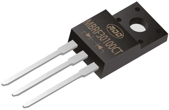
Schottky diodes are available in leaded and surface mount (SMD) packages. Schottky diodes in leaded packages are usually used as high-frequency high-current rectifier diodes, freewheeling diodes, or protection diodes. It is available in single-tube and pair-tube (dual diode) packages. Schottky pair tubes have three pin-leading methods: common cathode (the negative poles of the two tubes are connected), common anode (the positive poles of the two tubes are connected) and series connection (the positive pole of one diode is connected to the negative pole of the other diode).
Surface-mounted Schottky diodes have various packaging forms such as single-tube, double-tube and triple-tube types, and there are A~19 pin lead-out methods.
Advantages of Schottky Diodes
The main advantages of SBD include two aspects:
1) Since the height of the Schottky barrier is lower than that of the PN junction barrier, its forward conduction threshold voltage and forward voltage drop are lower than those of the PN junction diode (about 0.2V lower).
2) Since SBD is a majority carrier conduction device, there is no problem of minority carrier lifetime and reverse recovery. The reverse recovery time of SBD is only the charging and discharging time of Schottky barrier capacitor, which is completely different from the reverse recovery time of PN junction diode. Since the reverse recovery charge of SBD is very small, the switching speed is very fast and the switching loss is very small, especially suitable for high frequency applications.
However, since the reverse potential barrier of SBD is relatively thin, and breakdown easily occurs on its surface, the reverse breakdown voltage is relatively low. Since SBD is more susceptible to thermal breakdown than PN junction diodes, the reverse leakage current is larger than that of PN junction diodes.